Add your promotional text...

Unit - II : 8051 microcontroller
CA – 153 – T : Introduction to Microcontrollers First Year of B. Sc. (Computer Applications) - (2024 Course)
AICTE MICROCONTROLLER
Asst.Prof. G. A. Darandale
Features of 8051 Microcontroller:
8-bit CPU: Processes 8 bits of data at a time, making it suitable for simple control tasks.
Memory:
ROM (Program Memory): 4 KB on-chip ROM for storing programs.
RAM (Data Memory): 128 bytes on-chip RAM for data storage.
I/O Ports: Four parallel 8-bit input/output ports (P0, P1, P2, P3), each can be used as input or output and are bit-addressable.
Timers/Counters: Two 16-bit timers/counters for timing operations and event counting.
Serial Communication: Built-in full duplex UART for serial data transfer, allowing communication with other devices.
Interrupts: Five interrupt sources (two external, two from timers, one from serial port) to handle urgent tasks quickly.
Bus System:
8-bit Data Bus: For transferring data within the microcontroller.
16-bit Address Bus: For accessing memory locations.
Register Banks: Four register banks, each with eight 8-bit registers, for efficient data handling.
Special Function Registers (SFRs): Control various operations and peripherals of the microcontroller.
Oscillator and Clock Circuit: Built-in oscillator to provide the necessary clock signal for operation.
External Memory Support: Can connect to up to 64 KB of external ROM and 64 KB of external RAM if needed.
Power-Saving Modes: Includes idle and power-down modes to save energy during inactivity.
Bit and Byte Addressable RAM: Allows flexible data manipulation for control applications.
Other Features: Some versions include additional features like ADCs, DACs, and op-amps for advanced interfacing.
Block Diagram & Architecture of 8051:
The 8051 microcontroller is a single-chip microcomputer integrating a CPU, memory, I/O ports, timers, and serial communication on one chip. Its block diagram includes the following main components:
CPU (Central Processing Unit): Controls all operations, including the ALU (Arithmetic Logic Unit), Program Counter, Stack Pointer, Accumulator, and general-purpose registers.
RAM (128 bytes): Divided into register banks, bit-addressable memory, and scratchpad area.
ROM (4 KB): Stores program code.
I/O Ports: Four 8-bit parallel ports (P0, P1, P2, P3) for interfacing with external devices.
Timers/Counters: Two 16-bit timers/counters for timing operations.
Serial Port: For serial communication.
Interrupt Control: Manages six interrupt sources.
Oscillator & Clock Circuit: Provides clock pulses for operation.
Bus Control: Manages data and address buses for internal and external communication.
Internal Memory Organization:
The 8051 has a unique memory structure:
1. Program Memory (ROM)
Internal ROM: 4 KB for program storage.
External ROM: Up to 64 KB can be interfaced if needed.
2. Data Memory (RAM)
Internal RAM: 128 bytes, mapped from 00H to 7FH, split into:
Register Banks (00H–1FH): Four banks, each with eight registers (R0–R7).
Bit-Addressable Area (20H–2FH): 16 bytes, each bit can be addressed individually (128 bits).
Scratchpad RAM (30H–7FH): 80 bytes for general-purpose storage.
External RAM: Up to 64 KB can be interfaced for data storage.
3. Special Function Registers (SFRs)
Located from 80H to FFH (upper 128 bytes of address space).
Control and monitor various functions (timers, serial port, I/O, etc.).
Special Function Registers (SFRs)
There are 21 SFRs in the 8051, each 1 byte (8 bits) wide.
Examples include:
Accumulator (A), B Register
Program Status Word (PSW)
Port Latches (P0, P1, P2, P3)
Timer Registers (TCON, TMOD, TH0, TL0, TH1, TL1)
Serial Control (SCON), Serial Buffer (SBUF)
Interrupt Enable (IE), Interrupt Priority (IP)
Some SFRs are bit-addressable, allowing manipulation of individual bits.
PSW (Program Status Word) Register:
8-bit register reflecting the CPU status and control.
Bit functions:
CY (Carry flag): Arithmetic carry/borrow.
AC (Auxiliary Carry): For BCD operations.
F0: User-defined flag.
RS1, RS0: Register bank select bits.
OV (Overflow): Arithmetic overflow.
P (Parity): Even/odd parity of the accumulator.
Main Functions of the PSW Register:
Indicates the results of arithmetic and logical operations.
Controls which register bank (out of four) is currently being used.
Helps manage program flow based on the outcome of operations.
Description of Each Bit:
Carry Flag (CY): Set when there is a carry out of the most significant bit during addition, or a borrow during subtraction.
Auxiliary Carry Flag (AC): Set when there is a carry from bit 3 to bit 4 in an operation, mainly used in BCD arithmetic.
Flag 0 (F0): A general-purpose flag that can be used by the programmer for temporary storage.
Register Bank Select Bits (RS1 and RS0): These two bits select which of the four register banks (Bank 0, 1, 2, or 3) is active for use.
Overflow Flag (OV): Set when the result of an arithmetic operation is too large to fit in 8 bits.
Parity Flag (P): Automatically set or cleared to indicate if the number of 1’s in the accumulator is even (parity).
PSW is Uses :
The PSW is automatically updated after arithmetic and logical instructions.
Programmers can also set or clear some bits as needed for program control.
The register bank select bits allow switching between different sets of general-purpose registers, which is useful in interrupt routines or multitasking.
Importance of PSW :
It helps the microcontroller make decisions, such as whether to branch to a different part of the program based on the result of an operation.
It enables efficient use of resources by allowing quick switching between register banks.
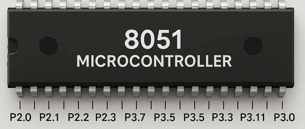
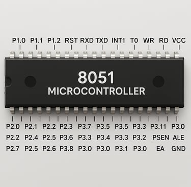
Pin functions of the 8051 microcontroller :
Port Pins
Pins 1 to 8: These are Port 1 pins (P1.0 to P1.7). They are used for general-purpose input and output operations.
Pins 10 to 17: These are Port 3 pins (P3.0 to P3.7). They work as input/output pins and also have special alternate functions like serial communication, external interrupts, timer inputs, and external memory control.
Pins 21 to 28: These are Port 2 pins (P2.0 to P2.7). They serve as general-purpose input/output pins and also provide the high-order address byte when using external memory.
Pins 32 to 39: These are Port 0 pins (P0.0 to P0.7). They can be used as input/output pins and also act as multiplexed address and data bus lines when connecting to external memory. External pull-up resistors are needed when used as I/O.
Control and Special Pins
Pin 9: This is the RESET pin. Applying a high signal resets the microcontroller.
Pins 18 and 19: These are XTAL1 and XTAL2 pins, which connect to an external crystal oscillator to provide the clock signal.
Pin 20: This is the GND pin and should be connected to ground.
Pin 29: This is the PSEN (Program Store Enable) pin. It is used to enable external program memory.
Pin 30: This is the EA (External Access) pin. It selects between internal and external program memory.
Pin 31: This is the ALE (Address Latch Enable) pin. It is used to latch the lower byte of the address during access to external memory.
Pin 40: This is the VCC pin and should be connected to the +5V power supply.
Summary
Ports 0, 1, 2, and 3 are used for general input/output and special functions.
The RESET, XTAL1, XTAL2, PSEN, EA, and ALE pins handle control, clock, and memory interface tasks.
VCC and GND are for power supply connections.
These pin functions allow the 8051 microcontroller to interact with external devices, memory, and perform its required operations efficiently.
Structure & Operation of I/O Ports:
Four 8-bit ports (P0, P1, P2, P3):
Port 0: Dual-purpose (I/O or multiplexed address/data bus for external memory). Needs external pull-up resistors.
Port 1: General-purpose I/O, internal pull-ups.
Port 2: General-purpose I/O or high-order address bus for external memory.
Port 3: General-purpose I/O and alternate functions (interrupts, serial, timers, etc.).
Operation: Each port can be programmed as input or output. Ports are bit- and byte-addressable, enabling flexible interfacing.
External Memory Interface:
Program Memory: Up to 64 KB external ROM can be connected. If EA (pin 30) is low, the microcontroller fetches code from external memory.
Data Memory: Up to 64 KB external RAM can be interfaced.
Control Signals:
PSEN (Program Store Enable): Activates external program memory.
ALE (Address Latch Enable): Latches the lower byte of the address from Port 0.
Port 0 and Port 2: Used to send address/data to external memory.
In summary:
The 8051 microcontroller features a well-organized architecture with integrated CPU, memory, I/O, and peripherals. Its memory structure separates program and data spaces, uses SFRs for hardware control, and supports both internal and external memory. The four I/O ports are versatile, and pin functions are designed for efficient interfacing in embedded applications.